Here are my schematic observation points after a few days of evaluating AI-64 for potential use in our projects (and some suggestions for next revisions, more like user wish list):
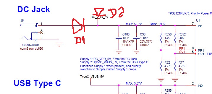
Power distribution circuitry - I would add x2 protection diodes for 5V feed from barrel connector and P9 (DC_VDD_5V signal). Rationale is a use case of having “something” like PoE for example, or 12V-24V buck converter, or battery as cape and “by mistake” connection to barrel feed. It’s just a good engineering practice. While one can add protection diode at cape level, there is no way to implement it at barrel connector.
See picture attached -
PCIe Key A/E slot has x2 PCIe lanes populated and it looks like correct placement for secondary PCIe lane RX/TX differential pairs (we still have to test it assuming that somebody will show how to turn it on). The only card that I know that uses this PCI-SIG optional provisioning is Google Coral dual TPU M.2 card and we will definitely test it. BUT, optional REFCLK for secondary lane is not populated, which leaves us with x2 lane interface configuration only, unless M.2 target will have clock fanout buffer implemented. So, I assume that this x2 lanes can be configured as x2 lane interface or two x1 lane interface with latter requirement for secondary REFCLK signal. I would keep options open and implement these secondary REFCLK differential pair if possible (unless it means addition of fanout buffer).
Since P9 is not a “standard” BB length and extends to USB 2.0 D+/D- signals taken from USB 3.0 HUB on board, why don’t we just extend it length to x4 more pins and route these USB 3.0 differential pairs? Having USB 3.0 at P9 (or extended P8, whatever works) would greatly extend cape ability to implement different “things”, like full blown LTE/5G modem, NVME implementation via well known JMicron chip offerings etc. etc. By taking a look at board layout it shouldn’t be a big deal - at least having these x4 signals somewhere on suitable header will do the trick. I would even have all of them on a header (x4 from M.2 related hub port, and x4 from P9 related hub port) - something similar to J10 will do. We can certainly use both for advanced capes.
I guess for 2) above idea would be to have a multiple options for these x2 lanes configuration. We do plan (preliminary) to create cape that will be “connected” to this M.2 slot through flat cable or flex pcb, and having x2 separate x1 PCIe interfaces will be definitely useful option for implementation, otherwise a small PCIe switch (Diodes or Broadcom/PLX) with refclk fanout will be required. Plans are to utilize this Gen 3 interface to maximum ability - we would love to have on this cape x3 A/E slots for Intel AX200/210 radios, x1 USB 3.0 LTE/5G modem and possible 2280 NVME.
btw - we will test NVME with BBAI-64 next week with Key A/E to Key M adapter (vertical) - do not expect any issues since Eval Board has it, so I assume it has been tested already. we would like to see what is bandwidth/throughput via single PCIe Gen 3 interface, and definitely will post results here.
QUESTION: are there any plans to implement a direct boot from NVME? Any plans for flasher to/from NVME?
Ok, let’s take it step-by-step. I will report our tests with (single lane) NVME and then we can think about how to make it graceful. I agree that having kernel and boot stuff at eMMC level and rootfs mounted on NVME is probably a way to go, we just will need a documented “recepie” that users can blindly follow. Adapter that we will be using in our testing is the following: M.2 NGFF nvme SSD to M.2 Key A/E Adapter (Vertical Installation) for 2280 Type SSD
Sintech are good overall, but we had an issue with their “ribbon” style cable in a past, plus they are really meant for Gen 2 speeds. Direct attachment should be able to demonstrate a “real” speed maximum figures. On the other hand, Sintech (as far as I remember) has another offerings that do have PCIe switch with 2 or 3 slots - probably can be used to mimic our intended design. Overall, idea is the following - x2 PCIe Gen 3 lanes in terms of bandwidth should be sufficient to run x3 WiFi6e radios plus BTLE plus LTE/5G modem. How dual core A-72 will be able to handle it is another story - experience shows that one usually saturates CPU much faster that saturating PCie, especially Gen 3 (1000MB/sec bidirectional, or 8Gb/s) - should be plenty of bandwidth, way beyond what dual-core ARM can handle.
Well, due to diode drops these would need to be “ideal” diodes. Certainly would be nice to have them, but they do take space and cost. I’ll see if we can’t fit them in if there is an update.
I have a lot of doubts if SuperSpeed could work over these connectors–that’s why I stuck to HighSpeed. Because we have a SuperSpeed hub, we do have extra SuperSpeed signals on the board, but I don’t think M.2 has a standard place to bring them across and the pin headers just don’t seem likely to work.
You are correct regarding a “simple” diodes that would present ~300mV forward voltage which in turn would violate USB prescriptive 5% tolerance at USB connectors (the rest of your circuitry should be just fine). I do understand that implementation of an ideal diode based on MOSFET with “ideal diode driver” will take a space and will add to cost. At least we (you) should outline somewhere in documentation (for future cape developers as well as for existent capes such as PoE) that souring 5V from cape simultaneously with power jack is strongly prohibited and will lead to damage (i.e. smoke and flame) - more likely at power supply/cape level, less likely at BBAI-64 level thanks to power mux with current limiting setting.
As for USB 3.0 - addition of USB 2.0 to cape interface is already a BIG deal which open a door to multiple designs that can utilize a plethora of different gadgets and silicons (like FTDI and alike), plus ability to implement an additional hub at cape level. It’s just a desire to have these USB 3.0 differential pairs that you do not use (like ones that belong to cape USB 2.0 port). For the connector/header I do no think it is a big issue (in case you can “squeeze” it somewhere) - main line legacy motherboards use this concept with even 0.1" headers for years without any problem. As I said, having USB 2.0 at cape level is already fantastic, but having 3.0 as well would be just a Cadillac. And yes, you can not provision USB 3.0 at Key A/E and be within standard, but you can certainly do it for Key B (x1 lane PCIe, USB 3.0, USB 2.0 etc.) but than it will change your design and will require Key B to Key A/E adapter board (not a big issue), but then again, if you do consider Key B then you probably do consider 3042, 3052 and 3060 form factor capability for mounting to accommodate all modern LTE/5G modems - in other words totally different animal. On the other hand, having two PCIe lanes at your current Key E connector does satisfy PCI-SIG standard, the only thing that I would have is secondary REFCLK in order to be able to configure x2 lane vs two x1 lane interfaces. BUT, on the other hand I do know only one M.2 Key A/E card in existence that has two lanes requirements, and it is dual Google Coral TPU card. btw - can somebody show me how to configure/enable secondary PCIe lane on BBAI-64 m.2 slot?
One more point to make (missed it last time) - since you do have now relatively powerful machinery under the hood, plus all this filtering capabilities with DSPs, and AI capabilities on-board, the very logical applications will be something like smart cameras, smart sensors etc. etc. - which in many applications will require PoE. Even though crafting PoE cape does not seem to be a big deal (Silvertel modules are very affordable option), it will require a jump cable between this PoE cape and RJ-45 on board. It would be much more logical and practical to use PoE capable RJ-45 with 4-pin header for power (something similar to what Raspberry Pi has). Should not add too much to BOM price, but will definitely be extremely practical for many applications.
On a second sought, what is original intent of DC_VDD_5V vs VSYS_5V0 at cape level? DC_VDD_5V can be treated as a) power source from cape to power the board and cape all together (assuming that barrel is not plugged), or b) power source from barrel to power board and cape in case cape requires current in excess what you power mux can deliver through VSYS_5V0 and sufficient power supply plugged to barrel to power both BBAI-64 and power hungry cape?
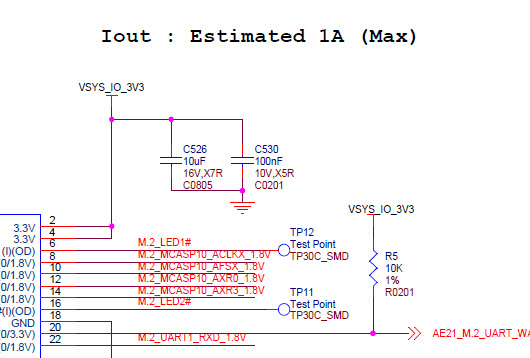
One more observation - it seems that power consumption at M.2 Key A/E (Type 1) is underrated base on what is prescriptive PCI-SIG M.2 electro-mechanical spec states. See below: