Hello all,
To suppplement the project I did this summer, I’m designing a cape (that will be released soon) to fit the BeagleBone Black that provides buffering between the Bone and the user hardware. It uses a 74LVCH16245 buffer for the purpose. I had two questions:
(i) Since the logic input pins are also the BOOTx pins for the AM3358 SoC, I wouldn’t like the cape to kick in before the SoC boots up. The reference manual states that “no pin is to be driven till SYS_RESETn is high” .
However on page 113 - “2) Do not drive any external signals into the I/O pins until after the VDD_3V3B rail is up.” caused a bit of confusion in my mind as to which criteria is more important and should be satisfied in this case.
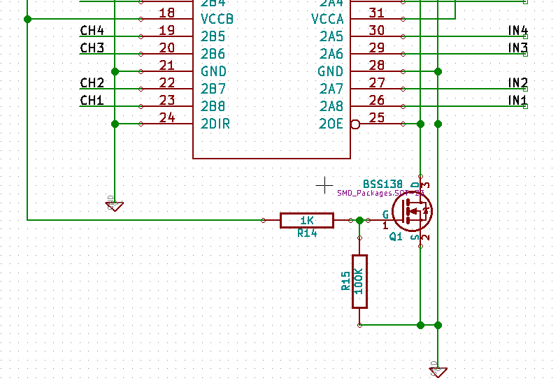
The current setup for this purpose is a BSS138 that pulls the OE of the buffer low when VDD_3V3B is present. The OE pin is high otherwise. I’ve enclosed an excerpt of the schematic in this post.
(ii) If there should be ~33 ohm resistors between the SoC I/O pins and the buffer, and between the logic inputs and the 74LVCH16245. Going through an appnote by TI I found that the 16245 integrates some form of termination on the I/O pads and think it may not be required in this case.
Best Regards
Abhishek
Hello all,
To suppplement the project I did this summer, I'm designing a cape (that
will be released soon) to fit the BeagleBone Black that provides buffering
between the Bone and the user hardware. It uses a 74LVCH16245 buffer for
the purpose. I had two questions:
(i) Since the logic input pins are also the BOOTx pins for the AM3358 SoC,
I wouldn't like the cape to kick in before the SoC boots up. The reference
manual states that "no pin is to be driven till SYS_RESETn is high" .
However on page 113 - "2) Do not drive any external signals into the I/O
pins until after the VDD_3V3B rail is up." caused a bit of confusion in my
mind as to which criteria is more important and should be satisfied in this
case.
The current setup for this purpose is a BSS138 that pulls the OE of the
buffer low when VDD_3V3B is present. The OE pin is high otherwise. I've
enclosed an excerpt of the schematic in this post.
I would recommend powering your buffer from the 3.3V power rail made
available for the VDD_3V3B rail and using the SYS_RESETn signal as an
output enable (it's safe to drive the pins when the reset line is high).
(ii) If there should be ~33 ohm resistors between the SoC I/O pins and the
buffer, and between the logic inputs and the 74LVCH16245. Going through an
appnote by TI I found that the 16245 integrates some form of termination on
the I/O pads and think it may not be required in this case.
The only reason to put series resistors between the driver and the SoC
would be to control reflections. Whether you need these or not depends
on the edge rate of the driver and the overall trace length. Since the
LCD/HDMI pins already have small capacitors on them on the BeagleBone,
an additional series back-termination resistor is almost certainly
unnecessary. You might need something for the pins that aren't part of
the HDMI interface, but that's mostly going to depend on the edge rate
of your buffer (signal ringing is related mostly to the dI/dt of the
signal edges, and not so much the overall signal frequency).