There’s a few ‘gotchas’ with following the docs when it comes to customising the FPGA on this awesome little board, so I thought I’d go through the walkthrough on video, and then extend a bit further past it with slightly more Verilog and logic complexity to show how easly you can tinker with things!
Very well done walkthrough taking you through the entire gateware process. Congrats!
Thanks mate, took some time to work it out! And thanks for your input too
Cheers mate, glad it’s still helping people this much later!
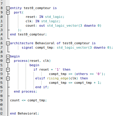
First of all, your work is amazing! I’m new to using the BeagleV Fire and I’m using Libero SoC to generate the bitstream. I started with a simple example, a counter, and I want to connect the outputs to LEDs 1, 2, 3, and 4. However, I’m not sure what to write in the constraint file to achieve this because I can’t find the pin names for the user LEDs. If you could help me, I would be extremely grateful.
Thank you in advance,
Welcome @j-a-s-22.
Depending on the configuration you want, they’re in here:
sources/FPGA-design/script_support/components/CAPE/<config>/constraints/cape.pdc
F. ex. DEFAULT
I believe what you’re looking for could be:
set_io -port_name P8_PIN3_USER_LED_0  \
    -pin_name V22       \
    -fixed true         \
    -OUT_DRIVE 12       \
    -RES_PULL None      \
    -DIRECTION INOUT
as an example, but I’m un-sure why you would want to change it.
If you want to connect to any of the defined pins, you do so by making sure the port
in your top SD is named correctly.
Note, some of the wires are brown, signifying that they can’t be changed.
That can be because they’re connected to a BIBUF macro somewhere,
but I think you can still change the port name, not that you’d want to.
If you look at either @platima’s video or here:
you can see how we "cut* the original GPIO busses and hijack the pins that way.
i can’t connect the count[0] to the V22 : Location is illegal. i tried to make the connection with I/O Editor

Hang on! You did not start with the Gateware repo as your starting point, did you?
Are we looking at a completely blank design?
Should I ? hahah
I started with VHDL code and then moved on to the design phase. Next, I handled the routing using the I/O editor. After these steps, I’ll generate the bitstream and deploy it to the FPGA.
No no, of course not.
We just need to get certain assumptions right, like what “field” we’re playing on, etc.
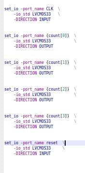
Can you create a blank constraints file and paste this in:
set_io -port_name count[0]  \
    -pin_name V22       \
    -fixed true         \
    -OUT_DRIVE 12       \
    -RES_PULL None      \
    -DIRECTION OUT

set_io -port_name count[1]  \
    -pin_name W22        \
    -fixed true         \
    -OUT_DRIVE 12       \
    -RES_PULL None      \
    -DIRECTION OUT

set_io -port_name count[2]  \
    -pin_name V19       \
    -fixed true         \
    -OUT_DRIVE 12       \
    -RES_PULL None      \
    -DIRECTION OUT

set_io -port_name count[3]  \
    -pin_name V20        \
    -fixed true         \
    -OUT_DRIVE 12       \
    -RES_PULL None      \
    -DIRECTION OUT
just to see how Libero reacts to that…
You didn’t specify how you think to deploy your bitstream. Do you have a JTAG programmer?
Ok. Would you mind sharing a bit more of your screen?
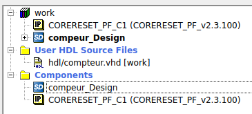
I particular, I need to see your design hierarchy…
Looks like your nets aren’t getting promoted to the outside.
Been looking at it some more and it turns out our particular pin V22 is in bank 0.
HSIO is normally running at 1.8V, so you have to remove the io_std from your 4 count pins.
If you right-click on say, count[0] you can select “unplace from location”. Do that.
Then on the Port View, open the I/O Standard dropdown and select LVCMOS18;
that should allow you to select pin V22.
You should do the same from your CLK and reset inputs,
and use the I/O Planner to make sure you get the right banks and voltages.
Make sure you tripple-check everything with the schematic,
because getting I/O Standards and bank voltages wrong, is exactly what can destroy your Beagle.
You have been warned! You are proceeding on your own risk here…
Also, you did not say if you have a JTAG programmer or not.
If you go ahead and program your design as is, you will not be able to boot back into Linux
and restore the functionality. There’s no MSS to run anything right now.
Thank you for your patience! I have asked you many questions, but this will be the last one, I promise xD ! Could you please help me find the pin for the reset button? I want the program to start from 0 when I click the reset button, but I can’t find the FPGA number associated with this .

.No, I thought I was going to deploy the design directly on the FPGA!
Nonsense; that is what we’re here for.
The complete schematic is here:
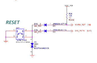
The button you’re looking for is here:

and that puts it on pin W12 and H7 (W12 might be your best bet though).
I am still not completely comfortable with your idea of deploying via FPGA,
because the current design will not be able to update itself.
Basically, you get to program your blinky, but then you’ll be stuck, unless you have a
FlashPro or another Beagle, in which case you can use DirectC and program the FPGA that way.
I’m not trying to be pedantic here, I just don’t want you to get stuck with no way out.
I’M GRATEFUL ! You help me so much (and saved me xD) ! I’m gonna think about it carefully
Keep in mind I do not have this board and don’t have a clue what I am writing about regarding board specifics.
I can say that you need to look at the .dts base file, pin mux file and if any overlays are used look at that source.
You will have to go in the pin mux and dig out the ball used, then look at its alias if assigned an alias. It requires some digging but bottom line is you need the actual ball number. Because, you can look up the mux, some options are not available on every pin. The mux is very limited, due to how the board designer envisioned the final design. You need to correlate ball(pin) number on the SoC to the actual physical pin on the header, if you don’t it will be not so much fun.


