Mapping PRU GPIO to chip pins to Cape Pin positions on a BBAI-64

I’m trying to figure out how to relate the various GPI and GPO bits in the PRU_ICSSGs to the pins on the Cape Headers. There’s a few different layers to doing this and here’s what I think I need to be doing. And I just need a sanity check to make sure I’m on the right track and determine if perhaps there’s a better strategy that someone with more experience can suggest.

I started with the BBAI-64 hardware documentation where the various connections are documented.
The chip-to-cape header I believe I found in the hardware documentation for the BBAI-64 here (p25):
BeagleBone_AI-64_Rev_B1_SCH_220602.pdf
(p25)
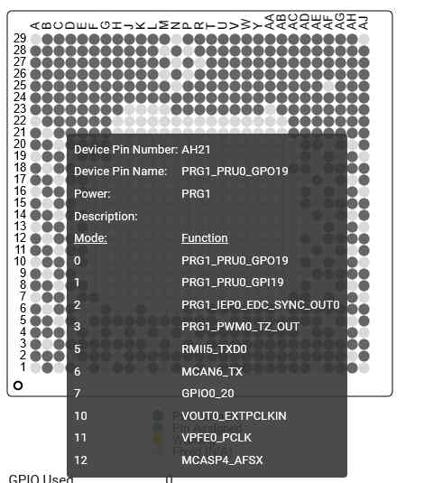
However the pin-names for each pin position seem to be logical names assuming a specific mix-combination. But their prefix does look like a pin-position ID. But just for curiosity, I search the document for the label name just to see where else they show up. I started with AH21_MCAN6_TX, which is labeled as Pin 3 on Header P8. Searching AH21_MCAN6_TX, it appears to be associated with something called PRG1 and wires to that as PRG1_PRU0_GPO19 / AH21.
This looks promising, but I’m still not sure I fully understand what I’m looking at. What is PRG1 (and PRG0)?

Assuming that AH21 is a pin-descriptor, I go to Sysconfig to see what it looks like, and sure enough AH21 correlates to a pin.

This is both confirming that the things I’m seeing are aligning. But I’m still not sure I fully know what PRG1 and PRG0 or if I need to care yet.

I do see the various Modes this pin can be put in and I see that putting it in Mode 0 makes it a PRG1_PRU0_GPO19 pin which sounds like what I would want. But I don’t know which PRU_ICSSGx peripheral this goes to. Is there a correlation between PRU_ICSSG1 and PRG1? If so, then this is a clue that I need to take care in picking pins that are all on the same PRG to keep all my pin selections within the same PRU_ICSSG subsystem.

Finally, I need to find the documentation that correlates each PRU’s GPO and GPI Register-bits to these pins. I remember reading this a while back for PRU_ICSS on the BBB, but I’d assume the mappings are all different for this platform. Given TI doesn’t claim support for the PRUs in the TVA4VM, how do I find documentation to complete this final step?

All that said, once I get some of these mysteries cleared up, I think I can move forward picking pins with a bit more confidence.


Background on the project I’m trying to prototype:
For the project I’m trying to prototype using the BBAI-64’s PRUs, to interface on an old 16-bit processor’s memory bus as a slave device (emulating PROM). The bus has 8 data/address lines, and 5 control lines. I need at least 8 bi-directional (high speed) pins for the data I/O. When the BBAI-64 is a slave, the 5 control pins will be monitor-only. However there is a scenario where the BBAI-64 will need to disable the processor and become the bus-master, and thus it will be controlling those lines. However in this scenario, timing is not nearly as critical since the BBAI-64 gets to set the pace (as the master). So handling this scenario outside of the PRUs is a completely viable option. Latency and timings are not nearly as critical and in this mode since all that’s being done is getting a memory-dump of the existing PROM.

I say all this in hopes that maybe there’s a similar BBAI-64 project already started that might have some similar pin-muxings already setup and some documentation of what cape-pins map to what Input and Output bits in which PRUs.

Also any documentation that details how to incorporate SysConfig information into a project (e.g. what are the muxing registers in the TVA4VM)? I’m sure a lot of this depends on when and where the muxing is being performed. For instance performing muxing as part of uboot launch will have different details than performing muxing at runtime as part of a fundamental application mode-switch. But any details that can be shared of helpful hints and things to be aware of might prove useful. For instance, I suspect accessing raw memory when your code is separated by the MMU where RAT is performed might have challenges and thus some helpful details as to how to defer/relay your need to read/write raw memory from those perspectives.
I think from reading some documentation on the PRUs, that they consist of 2 cores. Only one has the direct I/o connection. That would be my guess for PRG1.

If you can find that documentation, that would be interesting to look at.

Looking at the names on the various header pins for the BBAI-64, there are pins with all 4 of these name prefixes:
PRG0_PRU0_GPOxx
PRG0_PRU1_GPOxx
PRG1_PRU0_GPOxx
PRG1_PRU1_GPOxx

This would suggest that both cores (PRU0 and PRU1) in both PRU subsystems can map to GPIOs (assuming PRG0 = PRU_ICSSG0 and PRG1 = PRU_ICSSG1).

Either that or the naming convention is just unfortunate.

Page 8 in https://www.ti.com/lit/ug/spruj61/spruj61.pdf clarifies the “not supported features” of the PRU in J721E.

Hi,

there was another discussion about it - Question - Is AI-64 currently shipping with production processor (and no PRU)
I’m trying to run some PRU examples too, with PRUCAPE and until now I coudn’t run yet - I’m confuse about how to configure the pins - I believe I need to do a specific DTO with the pins enables - mainly because there is a robotic cape for the BBAI64 - so if there is support for the robotic cape I believe the PRU is present and working with the BBAI64.

From that document you linked to:

PRU-controlled GPIOs are features I’m planning to make use of, so this is very relevant and significant information for me.

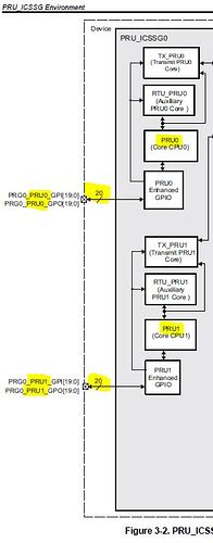
So it says 12 enhanced GPIs and GPOs. But which ones? According to Fig 3-2 (pg10 of this same document), there are 20 GPIOs that tie to those registers. Lower 12, upper 12? Anybody know or will this have to be figured out empirically? The brackets show [31:20] which would suggest the upper 12. However there were only 20 to start with and I didn’t think they extended all the way to 31. Regardless, as long as there are still 8 GPIOs that are working, that’s still OK for my needs. But knowing which bits are the active ones would be useful information.

It says specifically these are not supported in PRU0 for both PRU_ICSSG0/1. But what about PRU1? According to that same figure there’s supposed to be 20 on it. I can assume those are all present, correct?

Also the use of the word “enhanced” seems significant. Does that mean the new low-latency bi-directional support for GPOs that was introduced as part of the PRU_ICSSG subsystem? Or does this mean those GPIOs are unavailable/inoperable even using the pins the way the old PRU_ICSS did (as dedicated 1-directional GPIs or GPOs)? For those not familiar with the GPIO bi-directional enhancements I’m referring to, refer to this thread:
PRU_ICSS vs PRU_ICSSG wrt GPIO and bi-directional communications

I’m starting to see now why TI decided to just drop support for the PRUs in their official documentation so they didn’t have to clarify all these details.

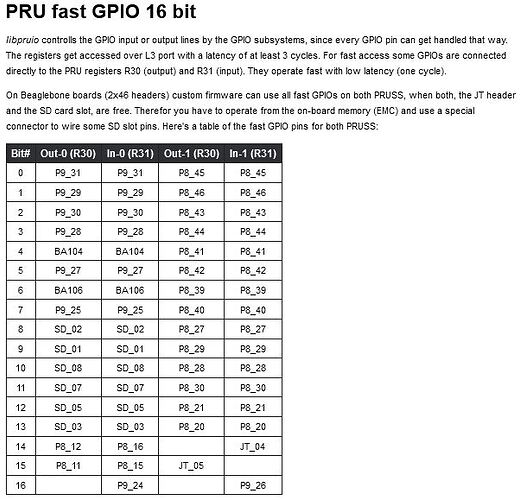
There are 16 fast GPOs for each PRU, and 17 GPIs (1 cycle latency). In order to make them floating, you’ve to change pinmuxing (interacting with a kernel module in order to write Control Module registers). Only on PRU-0 all of them are available on connectors (including SD-card slot). For PRU-1 16 GPIs and 15 GPOs are available. Find details at https://users.freebasic-portal.de/tjf/Projekte/libpruio/doc/html/_cha_t_n_t.html#SecPruGpio

The new PRUSS_ICSSG feature belongs to the DIGIO block in the PRU-IEP module. Both PRUSS can control the same 8 lines (2 cycles latency) at

Bit-0: P9_18
Bit-1: P9_17
Bit-2: P8_27
Bit-3: P8_29
Bit-4: P8_28
Bit-5: P8_30
Bit-6: P8_24, P8_39
Bit-7: P8_20, P8_40

on the BBB hardware. I guess the AI is pin-compatible.

Regards

I suspect there is some differences between pins-to-PRU-bits. From your linked website:

However my efforts to pick pins, resulted as follows:

Lines			uP-PIN	Logical Pin Desc		BBHeader
D0				AE29	PRG0_PRU1_GPO0			P8_31	
D1				AD28	PRG0_PRU1_GPO1			P8_32
D2				AD27	PRG0_PRU1_GPO2			P8_43
D3				AC25	PRG0_PRU1_GPO3			P9_15
D4				AD29	PRG0_PRU1_GPO4			P8_41
D5				AB27	PRG0_PRU1_GPO5			P8_42
D6				AC26	PRG0_PRU1_GPO6			P8_39
D7 				AA24	PRG0_PRU1_GPO7			P8_40

STB				AA28	PRG0_PRU1_GPO8			P8_27
DI				Y24		PRG0_PRU1_GPO9			P8_28
IT				AA25	PRG0_PRU1_GPO10			P8_29

BS0				AG26	PRG0_PRU1_GPO11			P8_30
BS3				AF27	PRG0_PRU1_GPO12			P8_14
	
RESET			AF28	PRG0_PRU0_GPO0			P9_28
MRESET			AE28	PRG0_PRU0_GPO1			P9_30
EEPROMDISABLE	AE27	PRG0_PRU0_GPO2			P9_12
PAUSE			AD26	PRG0_PRU0_GPO3			P9_27

TUNESEL0		AD25	PRG0_PRU0_GPO4			P9_15
TUNESEL1		AC29	PRG0_PRU0_GPO5			P8_40

You can ignore the 1st column, but what I’m focusing on is how the BB Headers relate to the Logical Pin name. I’m ASSUIMIG that, for example PRG0_PRU1_GPO0 correlates to Bit0 of R30 in PRU0.

Following that pattern, it appears the bit-for-bit relationship isn’t the same. Either that or I didn’t do as good of a job creating this table.

The other concern I have that I’ll need to sort out is that on the BBAI64, I can use the SD card slot simultaneously with these Pins. The application I have in mind will be logging a LOT of data, and I don’t want that logging to be on the eMMC. I’d rather it be on a “disposable” SD card.