I ordered the ULN2003 to test. CMOS was only available on the ULN2002…
So, my error. I will start with no EN and only OPTO but…
The issue is that if I want to disable the drive, I cannot without OPTO and EN together with OPTO then being a GPIO.
Seth
P.S. Should OPTO be a GPIO pin anyway? Now, that I see the Bold Face typing. I will not attempt to connect the GND of the Beagle to the DM332T EN terminal connector. Also, thank you for those resources.
Update
I forgot to mention… I also got a couple level translators that can handle voltage translation of a unidirectional type (CD40109BE). I think this one should prove valuable on another circuit or two…
You can add ENA back after you have it stepping and can be controlled in the same way DIR and PUL. It is just one less variable to worry about to start with.
As a test you can do the following.
connect motor and motor power only - the coils should be energised and stiff to turn.
now from Beagle (or any 5V source), connect 5V to OPTO and connect ENA to the 5V ground from the 5V supply(beagle). That should disable the driver and motor coils should not be energised and motor will be easy to turn.
Okay…thank you. I will test DIR and PUL only at first. I then will test EN once I can get the stepping done.
Also, If EN is GND, OPTO needs to be GPIO I think from what I read. Anyway, I will test every situation now and further into my findings. Simple things get past me…
This makes me error prone for randomness. So, I am still learning here. I need to read more of the datasheets, reference them when possible, and then accumulate educated decisions.
So far, I tested some pin outputs and just ran some source instead of getting to know the ULN2002 datasheet better. CMOS with a level translator that reports TTL output. Blah.
Seth
P.S. No wonder I was becoming angered by my actions. Blind running of source is not so healthy on the senses. And yes, the excited motor happens when EN is not attached but OPTO is a 5v GPIO. I think, and I am pretty sure from what I read, OPTO needs to be GPIO if and only if the EN terminal connector is used and connected to GND which makes an ON/OFF for driver usage, e.g. not for regular GPIO usage to toggle with time.
I feel welcomed, silly, and overwhelmed. I was using a CMOS chip when I needed TTL output for the ULN because of translation. Blah. Man, I am still not over it.
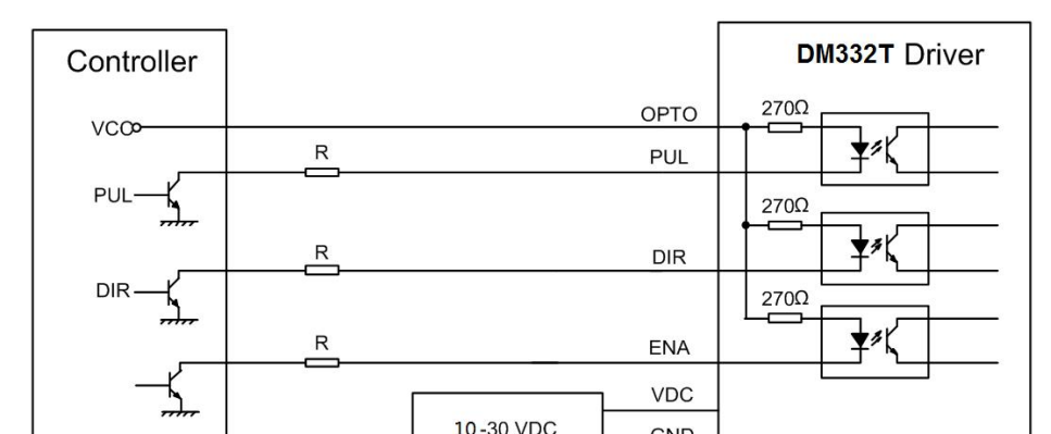
No OPTO should be connected to 5V. You can connected it to more than 5V but then you need to add extra current limiting resistors to the DIR,PUL and ENA signals or you will blow the opto iosolators.
It should be noted here that our DM320T and DM332T drivers do not have an ENA- terminal.The controller’s enable signal output needs to be connected to the OPTO public portwhen connected. At this time, OPTO is equivalent to ENA+.
Seth
Update:
Is an enable signal another word for GPIO or is it voltage and current? Strict guidelines should have been set on the allowancing of whomever wrote it. I mean…forget it. I am jibber jabbering. Off to look up ideas aboutu enable signals. Ben, see this:
I know it is just about an Enable Signal but when I think of Enable and GND, I think of GPIO for instance. So, there was a enabled peripheral and a GND. Right. And in this case, the GPIO is the enable pin.
This clearly shows that the enable pin should be switched to GND to enable/disable the driver. No ambiguity here. This is how I would expect it to work.
However the text you link to from the same company contradicts this. and claims there is no connection to the cathode of the opto isolator, but that the ENA pin is actually connected to the anode of the opto isolator But if that is the case where is the cathode of the opto isolator connected ?
It should be noted here that our DM320T and DM332T drivers do not have an ENA- terminal. The controller’s enable signal output needs to be connected to the OPTO public port when connected. At this time, OPTO is equivalent to ENA+.
I think basically what they may be saying here is that there is no enable signal really and you need to switch the OPTO power off to prevent pulses stepping the motor.
But if this case I would assume that the coils are going to always be energised as there is no signal to turn them off. No power on the OPTO pin just means the opto isolators won’t work.
This of course then contradicts their whole paragraph about disabling the driver to save power.
I think either their FAQ is wrong or the datasheet is wrong.
I would be very interested to see what is inside of the driver module.
I connected COM and VOLTAGE from the DMM to the OPTO and EN pins on the driver (DM332T).
Either omc-stepperonline has documentation issues or the translation for whatever language to English got mismatched or something.
I say those ideas because when COM is on EN and Voltage is on OPTO, I receive the NULL reading on my DMM. When switched, the voltage then reads an output.
And A-okay about the non-excited motor. When the driver is on PWR/GND from the bench supply/PSU, the motor stays excited. Okay…I am going to unscrew the screws and photograph the driver for you!
I think the reverse polarity at OPTO and EN is fair game for us digging into this driver.
Seth
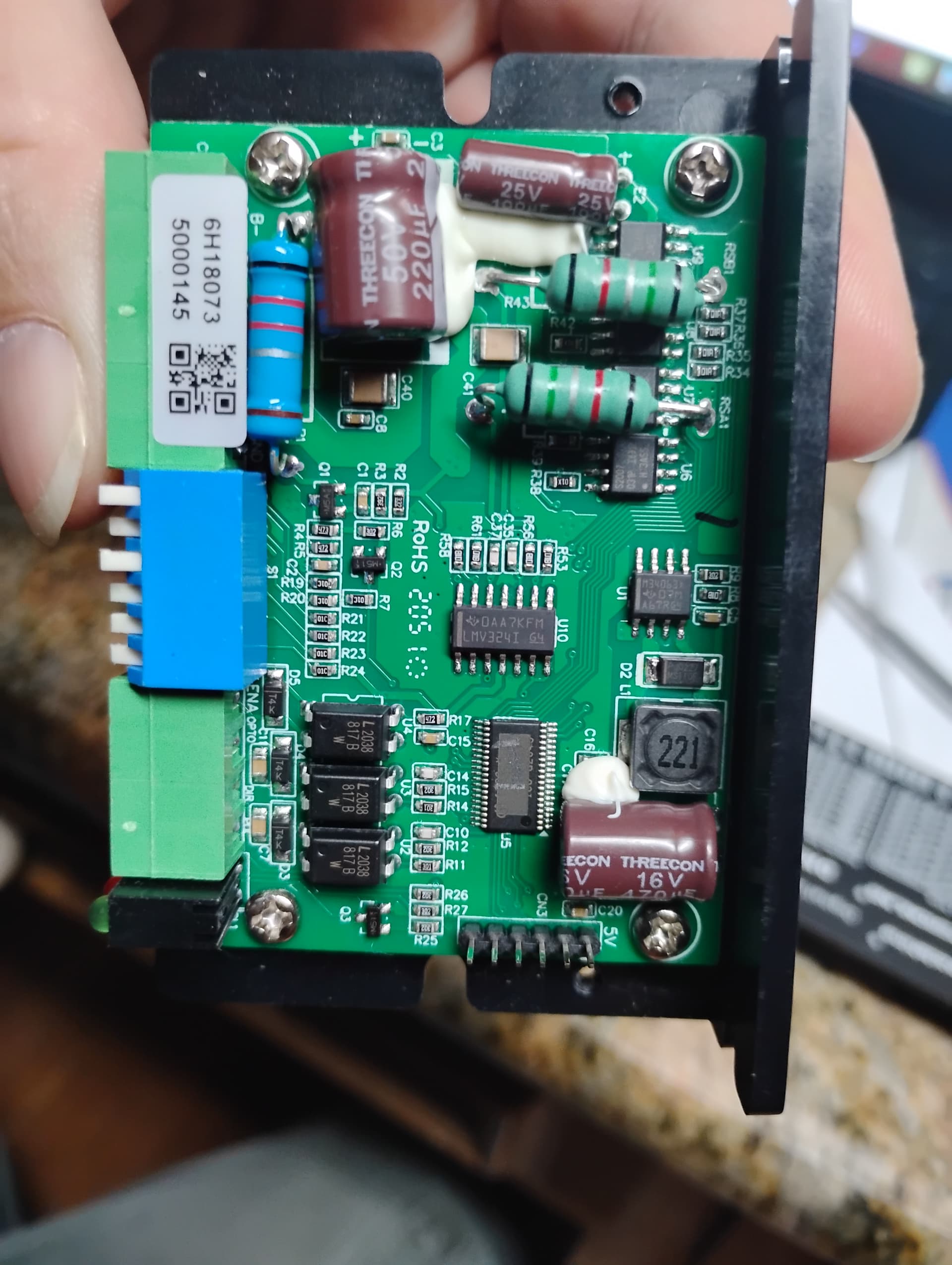
Here!
I think they have some TI chips on it. I need to zoom in…I will take a better photo soon.
OK thats interesting. Can’t find a datasheet for the optos, but at least it has 3.
I reckon the DM332T datasheet is probably correct and I would ignore the text in the FAQ. Maybe at some point they changed the design of the driver but didn’t update the FAQ.
But if you want to double check, with a DVM on resistance.
Pin 1 on the optos should measure around 270 ohms to the OPTO pin. Interestingly the current limiting resistors on the bottom of the PCB appear to be 270 ohms (ENA) and 300 ohms (DIR & PUL) The datasheet has them all at 270 ohms.
If you check pin 2 of the optos, they should be connected to the edge connector. Looks like they have some diode protection and in the case of the DIR and PUL signals a capacitor.
I can see there is a buck converter in there, probably 5V as the LMV324 is a quad op-amp, max 5.5V supply. Probably used for current sensing. Can’t tell what the actual driver chip is.
No I would supply the OPTO from the 5V on the Beagle otherwise you lose the opto-isolation.
Also if you used the 5V on the header, you would need to provide a common GND again losing the isolation.
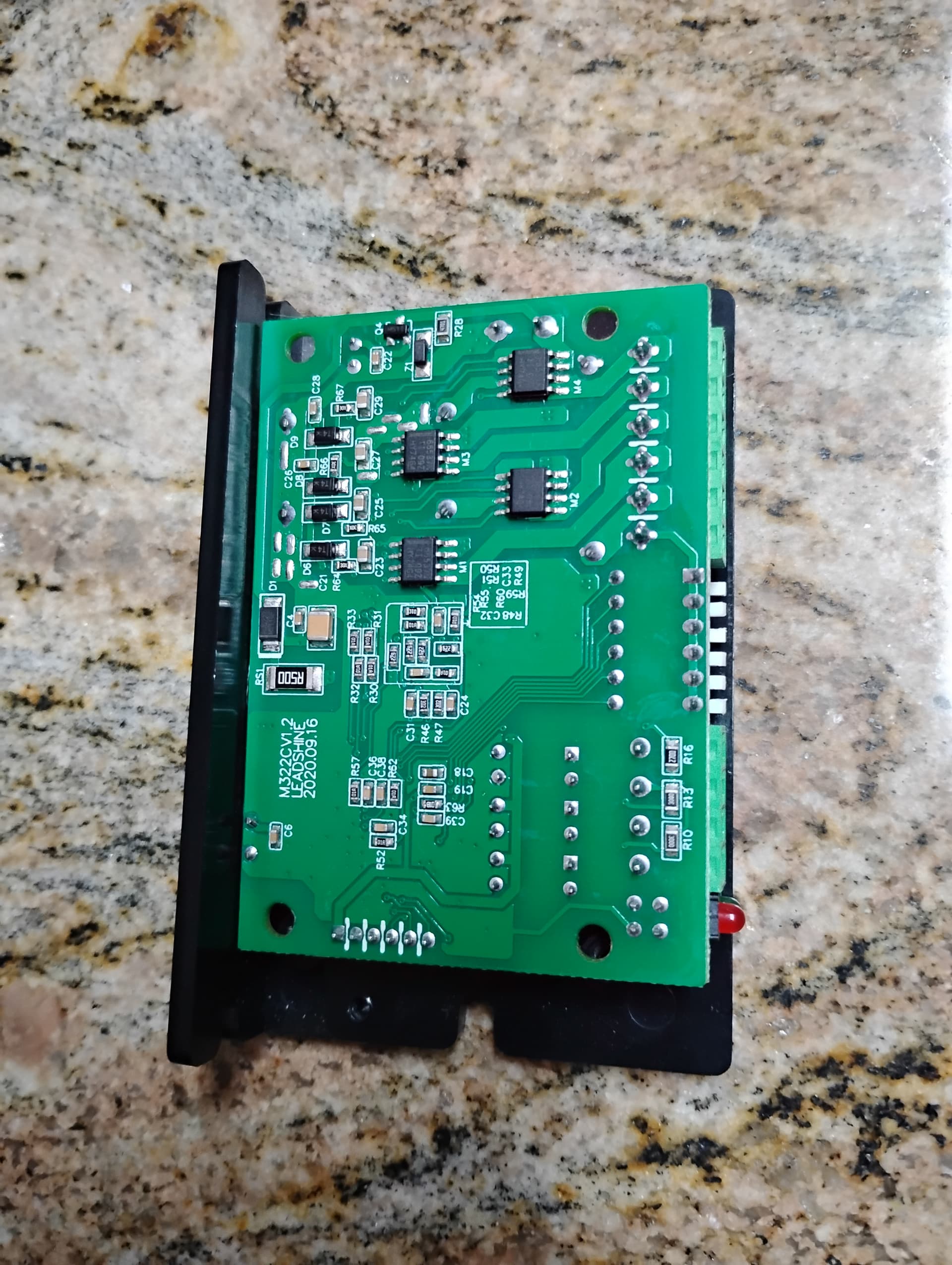
My guess is that 5V is from the internal buck converter and the header is probably used for testing the module because that 5V line goes the the driver side of the opto-isolators. Also looking at the PCB, the other header pins disappear under the driver chip, so almost certainly for testing the module after production.
The main chip with the label is the driver chip.
I assume the 4 chips in the top right of the PCB are to do with current sensing.
Probably a bit border line if the chip would work. According to the datasheet an input high needs to be a minimum 3.15V when VCC is 4.5V. It might work though as often chips will work outside the min/max specs. If you have nothing better to do, you can always wire one up and check with a scope to see if the outputs are toggling. Looks like it will sink max 25ma, so good enough for the optos.
Right, I saw that in the data. And yes, borderline is right.
The Y-AI cannot handle the mA and voltage output needed with the level shifter alone. 4mA is not enough and that is if it can handle that much mA at all.
I tested the GPIO output before and after the level shifter while running source without using edges, i.e. just HIGH and LOW.
While the source was in a hanging mode, meaning waiting for input, the voltage was in a state. I guess high impedance was its state. It was much lower than 3.3v before the level shifter and again after the level shifter at 5v.
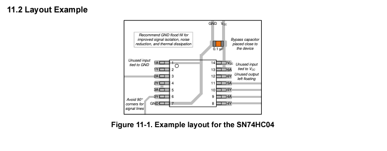
So…testing the SN74HC04 is an okay chip for testing alone. I do not see why with the driver in question. It seems 5v is needed on inputs (OPTO, DIR, PUL) on the driver and blah-blah-blah.
At times I feel like I am jabbering. And yes, Ben, the 25mA max from the hex inverter is nifty. Way more mA than the driver would ever need is how I see it.
I am just not sure now how to incorporate the mathematics of formulas to support the finding/research.
I mean…I read the data and I see it but they are missing lessons of useful information. For instance, (R = V / I) is a simple resistance equation but there is usually more to chips than finding the resistance via (R = V / I). It is usually way more complicated. I was reading capacitor logic math for formulas and equations. Blah! I had to stop. I was ill-prepared.
Anyway, I think the level shifter until further testing is done is not a “On Its Own” type of use case.
But, I can test it too!
Hmm. What happened? I thought you were going to try to set up a stepper with a chip…
Seth
P.S. I gave out the kernel and image. Argh…ha. I am sorry about the boards. hopefully, you can situate them again to better suit the needs of your ideas or for use cases. Enjoy…
That is my thoughts on that too. The one was working fine the other had issues but both had video, both were on the shelf until now. Am I missing something with the video adapter?
No clue. I tried a display and failed with the CSI0 and CSI1 ports on the board. I went back to basics!
Of course, the adapter from the Y-AI to the Camera module may be lacking in pinouts. I might get a new adapter… Of course, that is low on the wants/needs right now.
I went back to the early image to see what is going on and it did not have any video either, it was starting to smell. Got this image running, suspect the newer one would have the same.
debian@BeagleBone:~$ uname -a
Linux BeagleBone 6.1.80-ti-arm64-r58 #1bookworm SMP PREEMPT_DYNAMIC Sun Jun 23 01:29:22 UTC 2024 aarch64 GNU/Linux
debian@BeagleBone:~$
I will look at your project this evening.
What pins are you going to use, here is what is on this board:
debian@BeagleBone:~$ gpioinfo gpiochip0
gpiochip0 - 24 lines:
	line   0:      "GPIO8"       unused   input  active-high
	line   1:      unnamed       unused   input  active-high
	line   2:     "GPIO11"       unused   input  active-high
	line   3:     "GPIO10"       unused   input  active-high
	line   4:      "GPIO9"       unused   input  active-high
	line   5:      unnamed       unused   input  active-high
	line   6:      unnamed      "reset"  output  active-high [used]
	line   7:     "GPIO23"       unused   input  active-high
	line   8:      unnamed     "enable"  output  active-high [used]
	line   9:      "GPIO7"       unused   input  active-high
	line  10:     "GPIO24"       unused   input  active-high
	line  11:      unnamed       unused   input  active-high
	line  12:      unnamed       unused   input  active-high
	line  13:  "HDMI_RSTn"       unused   input  active-high
	line  14:  "HDMI_INTn"       unused   input  active-high
	line  15:      unnamed       unused   input  active-high
	line  16:      unnamed       unused   input  active-high
	line  17:      "GPIO3"       unused   input  active-high
	line  18:      "GPIO2"       unused   input  active-high
	line  19:      unnamed       unused   input  active-high
	line  20:      unnamed       unused   input  active-high
	line  21:      unnamed       unused   input  active-high
	line  22:      unnamed       unused   input  active-high
	line  23:      unnamed       unused   input  active-high
debian@BeagleBone:~$ gpioinfo gpiochip1
gpiochip1 - 87 lines:
	line   0:      unnamed       unused   input  active-high
	line   1:      unnamed "MIPI_SWITCH_OE" output active-high [used]
	line   2:      unnamed "MIPI_SWITCH_SEL" output active-high [used]
	line   3:      unnamed       unused   input  active-high
	line   4:      unnamed "regulator-3" output active-high [used]
	line   5:      unnamed       unused   input  active-high
	line   6:      unnamed       unused   input  active-high
	line   7:      unnamed       unused   input  active-high
	line   8:      unnamed       unused   input  active-high
	line   9:      unnamed       unused   input  active-high
	line  10:      unnamed       unused   input  active-high
	line  11:      unnamed        "PWR"  output   active-low [used]
	line  12:      unnamed        "ACT"  output  active-high [used]
	line  13:      unnamed       unused   input  active-high
	line  14:      unnamed       unused   input  active-high
	line  15:      unnamed       unused   input  active-high
	line  16:      unnamed       unused   input  active-high
	line  17:      unnamed       unused   input  active-high
	line  18:      unnamed       unused   input  active-high
	line  19:      unnamed       unused   input  active-high
	line  20:      unnamed       unused   input  active-high
	line  21:      unnamed       unused   input  active-high
	line  22:      unnamed       unused   input  active-high
	line  23:      unnamed       unused   input  active-high
	line  24:      unnamed       unused   input  active-high
	line  25:      unnamed       unused   input  active-high
	line  26:      unnamed       unused   input  active-high
	line  27:      unnamed       unused   input  active-high
	line  28:      unnamed       unused   input  active-high
	line  29:      unnamed       unused   input  active-high
	line  30:      unnamed       unused   input  active-high
	line  31:      unnamed       unused   input  active-high
	line  32:    "USB_RST"      "reset"  output   active-low [used]
	line  33:     "GPIO27"       unused   input  active-high
	line  34:      unnamed       unused   input  active-high
	line  35:      unnamed       unused   input  active-high
	line  36:     "GPIO26"       unused   input  active-high
	line  37:      unnamed       unused   input  active-high
	line  38:      "GPIO4"       unused   input  active-high
	line  39:      unnamed       unused   input  active-high
	line  40:      unnamed       unused   input  active-high
	line  41:     "GPIO22"       unused   input  active-high
	line  42:     "GPIO25"       unused   input  active-high
# 13 is gpiochip1, pin 33 ---- GPIO27
# 15 is gpiochip1, pin 41 ---- GPIO22
# 16 is gpiochip0, pin 7 ---- GPIO23
From what I can tell now, all GPIO pins work at 3.3v and at 5v after the level shifter. This is the good news. The lack of datasheet research stalled me at first. I am reading them more and more…